Wednesday, September 30, 2015

A collection of navigation computers


Type D-4 Time Distance Computer


 Type MB-9 Air Navigation, True Air Speed, Wing Components, Supersonic Computer
 Type MB-1 Computer, Air Navigation True Airspeed and Altitude

 E-6B Computer; Aerial, Dead Reckoning


x

Friday, September 11, 2015

DEC PDP 11 boards (and a PDP 8 DAC)

M8043 4 way async
M8192 KDJ11-A

x
http://www.willsworks.net/pdp11/BOARDS.HTM
x

KDJ11-AA (M8192) 11/73 CPU Module

This is a two slot CPU module. Its the most advanced in the series to which I have had access. It does not contain either on-board bootstrap ROM nor a console SLU. I do not have any of the documentation, but someone (thanks John) was kind enough to send me the following jumper and led information. The memory managment unit, MMU is well described in Micronote 8 and Micronote 11. Micronote 6 talks about the differences between the 11/23 and the 11/73 while Micronote 4 discusses upgrade paths to the 11/73.
There are 4 leds visible on the back of the CPU board:
  d4 mem, d3 slu, d2 cpu, d1 odt


            \     /   M8192            \    /
          -----------------------^^^^-----------
         |                       ||||           |
         |                      D4  D1          |
         |                                      |
         |                                      |
         |                                      |
         |   E36 Microprocessor                 |
         |                                      |
         |               o-o  W9                |
         |               o-o                    |
                         o-o
                         o-o
                         o-o  W5
                         o-o
                         o-o
                         o-o
                         o-o  W1
         |                                      |
         |                                      |
         |                                      |
         |          E34          E13            |
         |         Cache        State           |
         |        Control      Sequencer        |
         |                                      |
         |_                 _                  _|
           |_______________| |________________|
                   B               A
INSTALLATION:
2.1 INTRODUCTION
This chapter discusses the considerations and requirements to configure and install a KDJ11-A module in an LSI-11 system. The module can be installed in systems using the extended LSI-11 bus backplane as well as existing systems that use one of the standard LSI-11 backplanes. The items that must be considered before installing the module are as follows.
1. Configuration of the user selectable features.
2. Selection of an LSI-l I compatible backplane and mounting box.
3. Selection of LSI-l 1 options compatible with the KDJ11-A.
4. Knowledge of system differences when replacing an LSI-11 processor
with the KDJ11-A module.
2.2 CONFIGURATION
The KDJ11-A has nine jumpers for the user selectable features. The locations of these jumpers are shown in Figure 2- 1 and their functions are described in Table 2-1 . A jumper is installed by pushing an insulated jumper wire (P/N 1 2-1 8783-00) onto the two wirewrap pins provided on the module.
Table 2-1 KDJ11-A Jumper Identification
Jumper    Function
w1    Bootstrap address bit 15
W2    Bootstrap address bit 14
W3    Power-up option selection bit 02
W4    Bootstrap address bit 13
w5    HALT trap option bit 03
W6    Bootstrap address bit 12
W7    Power-up option selection bit 01
W8    Wakeup disable
W9    BEVNT recognition
2.2.1 Power-Up Options
There are four power-up options available for the user to select. These options are selected by jumpers W7 and W3. The bits are set (1) when the jumpers are removed. A power-up option is selected by configuring W3 and W7, as described in Table 2-2. A description of each option is provided below.

Power-Up Options
Option    W3            W7            Power-Up Mode
0        Installed    Installed      PC at 24, PS = 26
1        Installed    Removed        Micro-ODT, PS = 0
2        Removed      Installed      PC at 173000, P5 = 340
3        Removed      Removed        Users bootstrap, PS at 340
Option 0: The processor reads physical memory locations 24 and 26 and loads the data into the PC and PS, respectively. The processor either services pending interrupts or starts program execution, beginning at the memory location pointed at by the PC. Option 1: The processor unconditionally enters micro-ODT with the PS cleared. Pending service conditions are ignored.
Option 2: The processor sets the PC to 173000 and the PS to 340. The processor then either services pending interrupts or starts program execution, beginning at the memory location pointed at by the PC. This option is used for the standard bootstrap.
Option 3: The processor reads the four bootstrap address jumpers and loads the result into PC. PC<11:00> are set to zero, and the PS is set to 340. The processor then either services pending interrupts, or starts program execution, beginning at the memory location pointed at by the PC.
2.2.2 HALT Option
The HALT option determines the action taken after a HALT instruction is executed in the kernel mode. At the end of a HALT instruction, the processor checks the BPOK bit 00 before checking the HALT option bit 03. If BPOK is set, the processor will recognize the HALT option, which is controlled by the W5 jumper. When the jumper is removed, bit 03 is set (1) and the processor will trap to location 4 in the kernel data space and set bit 07 of the CPU error register. When the jumper is installed, bit 03 reads as a zero and the processor enters the micro-ODT mode. If BPOK bit 00 is not set when the processor checks, the option is not recognized and the processor loops until BPOK is asserted and the power-up sequence is initiated.
2.2.3 Boot Address
The boot address jumpers selects the starting address for the user’s bootstrap program when power-up option 3 is selected. The state of the highest four bits, <15:12>, is determined by jumpers W1, W2, W4, and W6, respectively. A bit will be set (1) when the respective jumper for that bit is installed and the bit will be read as a zero when the jumper is removed. During the power-up sequence, the processor reads the address determined by bits <15:12> and forces the remaining bits to read as zeros. Therefore, the user’s bootstrap program can reside on any 2048 word boundary.
2.2.4 Wakeup Disable
The KDJ11-AA module has an onboard wakeup circuit to properly sequence the BDCOK signal. When jumper W8 is removed, the wakeup circuit is enabled and the module will properly sequence the BDCOK signal. The wakeup circuit will be disabled when W8 is installed and external logic must be used to properly sequence the BDCOK signal.
2.2.5 BEVNT Recognition
The LSI-11 bus signal BEVNT provides an external event interrupt request to the processor. This feature is disabled when the W9 jumper is installed and disables the line time clock register. When the jumper is removed, the BEVNT input is recognized and is under control of the line time clock register. Specifically, the signal is recognized by the module when bit 06 of the line time clock register is set (1) and is disabled when bit 06 is not set (0). The line time clock register address is 17 777 546 and is a read/write register.
2.2.6 Factory Configuration
The factory or shipped configuration is described in Table 2-3. The user should review these features and change them accordingly to match the requirements of the system using the module.

Factory Configuration
Jumper     Status             Function
W1    Installed    Bit 15 set (I)
W2    Installed    Bit 14 set (1)
W3    Removed      Selects power-up option 2
W4    Installed    Bit 13 set (1)
W5    Removed      HALT instruction traps to location 4
W6    Installed    Bit 12 set (1)
W7    Installed    Selects power-up option 2
W8    Removed      Wakeup circuit is enabled
W9    Removed      BEVNT register is enabled
DIAGNOSTIC LEDS
The module has four LEDs that monitor the status of the module. See Dl through D4 and are located on the edge of the module, as shown in above. The Dl LED is turned on only when the module is operating in the micro-ODT mode. LEDS D2-D4 are used with the diagnostics and run during the power-up sequence. These LEDs are turned on at the beginning of the sequence and are turned off upon the successful pass of the diagnostic. Each LED monitors a primary function of the module operation, as described below.
LED Functions

LED On Test Conditions   
Dl Micro-ODT is entered.   
D2 Module could not do a write and read transaction to the CPU 
        error register.  Indicates the microcode is not running.
D3 Module attempted to read location 17 777 560 and timed out. 
        Indicates SLU is not responding. 
D4 Module attempted to read location 0 and timed out or attempted 
        to read location 17 777 700 and did not timeout. 
        Indicates the memory system is not responding.


Probable System Failure
LEDs    
Dl D2 D3 D4 Probable Failure
X On On On CPU module
X Off On On LSI-11 bus
X On Off On CPU module
X Off Off On LSI-11 bus or memory
X On On Off CPU module
X Off On Off SLU module
X On Off Off CPU module
X Off Off Off Console terminal

PDP 11 backplane. new project


Column A


Column B

Column C
Orange wire goes to the pin next to SSPARE3 on the 10 pin connector block.
Column D

Power connector

+ 12 + 5, grounds, and -12 power connectors on a "berg" type strip.


Overall view (Plus an After the Battle)
 
Now need to figure out what backplane this is.  From what I've seen on Ebay from the same seller, this may be a small LSI 11/03 system backplane, since a cpu card + memory card is now listed for sale.  Hopefully can snag that and have a nice little system with what I've got.

This is a backplane for what appears to be an H9270 PDP 11/03 system.

See page 136 of this manual

http://manx.classiccmp.org/collections/antonio/dec/ek-lsi11-tm-003.pdf

Page 136, H9270 backplane and cage

Backplane signal list from Appendix B page 1


Below with E.1, Basic Daisy chain is a single system layout.


below is the single backplane as well as a two backplane lashup.


Pin assignments


x


x


Friday, August 21, 2015

DEC boards KDJ11-A (2) KDF11-A and Motorola MMS1132 128kW x 16 (can be 18) memory.

Four more boards from the gold scrapper.

MMS1132 Motorola Memory

Rear of MMS1132

The KF11 board below is marked with a Sharpie that it is BAD.  But it is the only one with the FP processor and MMU, so I'm hoping it works on the other KDF I have.
KDF11-A

For the following two boards, both KDJ11-A boards, the date codes are near end of 1983 and all of the edge pins are present.  Note the one in the next illustration has the unused pins omitted.

I didn't find a clear revision in the etch indicating this change, in fact both have identical numbers for the most part.
KDJ11-A

KDJ11-A


M8043


M8028 Async with Modem

M8192 KDJ11-A
KDJ11-A (Bitsavers) PDP 11/73


M8186 PDP 11/23 KDF-11A

Includes E57, MMU chip.

A-614 PDP 8 DAC
setups for processor boards

http://www.willsworks.net/pdp11/BOARDS.HTM

KDF11-AX (M8186) CPU Module

This is a frequently encountered two slot CPU board. It supports an 18 bit address space through an MMU (Memory Manage Unit). It does not include the bootstrap and diagnostic capability nor SLUs as does the M8189, normally one or more additional boards (see below) provide this functionality. ODT is built into the microcode.
 
            \     /   M8186  REV A    \    /
         --------------------------------------
        |             o-W19-o                  |
        |             o-W18-o                  |
        |                                      |
        |                                      |
        |   M  S  F  C    o-W17-o      o       |
        |   M  P  P  P               -W01-     |
        |   U  A  I  U                 o       |
               R  S       o             
               E        -W16-
                          o
                o-W15-o
                o-W14-o
                o-W13-o
                o-W12-o
                o-W11-o
                o-W10-o
                o-W09-o
                o-W08-o
                o-W07-o     o-W04-o
                o-W06-o                o-W2-o
                o-W05-o                  E2  <-   see note on W3

        |                                      |
        |                                E1    |
        |_                 _                  _|
          |_______________| |________________|
                   B               A

            \     /   M8186  REV C    \    /
         --------------------------------------
        |                                      |
        |             o-W18-o                  |
        |                                      |
        |                                      |
        |   M  S  F  C            o-W1-o       |
        |   M  P  P  P                         |
        |   U  A  I  U                         |
               R  S
               E

                o-W15-o
                o-W14-o
                o-W13-o
                o-W12-o
                o-W11-o
                o-W10-o
                o-W09-o
                o-W08-o
                o-W07-o     o-W04-o
                o-W06-o
                o-W05-o                  E2

                                       o-W03-o
                                       o-W02-o
        |   o-W16-o                            |
        |   o-W17-o                      E1    |
        |_                 _                  _|
          |_______________| |________________|
                   B               A


    Note one of my manuals has a fairly lengthy section on
    the Revision history.  Apparently there are slight differences
    in some of the jumper locations so if yours doesn't look
    exactly like those above, I hope its close.  The manual claims
    the revision number is stamped into the module handle,
    but mine has no such stamp.  ECO's included A0-A7 and
    C0-C3, although nothing below A3 was shipped.  There
    is also no revision B for some reason.

    These are typical wire wrap stakes, and a wire wrap could
    be used, but the factory installs a tin jumper.

    The one I'm holding in my hand now seems to be something
    between the boards shown above.  Apparently W18 is vertically
    oriented rather than horizontal as shown above, and there is
    no W02 or W03.  Maybe this makes it a revision A as the Service
    Manual says "On etch 'A' modules, W3 is installed by
    soldering a jumper wire from E2 pin 5 to E2 pin 15."
    However it does have W16 and W17 as indicated for a REV C,
    and a horizontal set of pins where W1 should be so it could
    be a REV C?

    Note Rev A above has an extra W19, and no W3.  W2,W16, and
    W17 are relocated, with W1 and W16 now being vertically oriented.
    Most of this doesn't matter a lot, cause you aren't supposed to 
    mess with these!

    In the tables below 'I' => jumper installed, 'R' => removed.
    All revisions list four jumpers as DEC reserved, and says
    jumper should be set at factory configuration.  W18 is
    revision specific.  
 
    Jumper    Name            Function       Factory Set
    W1        Master Clock    I = enable            I
    W2        Reserved        Factory Set           O
    W3        Reserved        Factory Set           I
    W4        Line event      O = enable            I
    W5        power-up mode   (see 1 below)         I
    W6        power-up mode   (see 1 below)         O
    W7        halt trap       O = enter ODT         I
    W8        bootstrap mode  I = 173000            I 
    W9-15     bootstrap adr   (see 2 below)         I
    W16-17    Reserved        Factory Set           I
    W18 (A)   Reserved        Factory Set           I
    W18 (C)   Wake up circuit O = enable            I

    1) Power up modes are defined by jumpers W5 and W6 
    mode                       W5    W6
     0    pc@24,ps@26          O     O
     1    console ODT          I     O 
     2    bootstrap            O     I 
     ie if you want it to use bootstrap ROM install W6
        if you want it to start up in ODT   install W5

    2) If W8 is out, W9 through W15 define the starting bootstrap
    address, if installed the standard 17300 (octal is used).
    W9-W15 correspond to address bits 9 through 15 respectively.
    In is a logical 1, out is a logical 0.

    The following diagnostic programs are mentioned:
    JKDBBO  CPU trap and EIS
    JKDABO  MMU  (requires KTF11-A option, ie MMU chip)
    JKDCAO  FPIS part 1
    JKDDAO  FPIS part 2

    Note the FPIS (Floating Point Instruction Set) was an
    option as was the MMU in some.  FPIS requires an MMU.


Monday, June 8, 2015

Peer Protocols 0500 Scsi Narrow capture card


This is a board we did at Peer Protocols.  It captures narrow 10 megatransfers / sec traffic on an 8 bit 50 pin bus.

It was an early design and only had the narrow connector sticking out the back of the PC, so you had to put it in the middle of the bus.  Not an unusual place to wire such a board, but sometimes lead to fun trying to have a fully functional bus.

Termination of course had to be at the ends, and frequently in early days there was no active termination for the ends of narrow ribbon cables.

The top board, was from a development system, the Peer 7000.  It was a narrow and wide general purpose SCSI development system.  It could be loaded with firmware to be either an initiator or a target in any scenario.  The fact this customer had two of them, and they have the differential back end means it was a very high end site.  That they had the 0500 capture card meant they were likely doing narrow development.

The connector on the top of the 702 board was for suppling power for the differential to single end conversion.  Differential in and out was on both connectors.  The black 50 pin connectors are connected bussed together, and allows you to do a true loop thru.  The rear wide 68 pin connector allows you to do wide 16  bit bus loop in and out.

The second board shows the one 68 pin connector on the bottom of the board.  The photo above doesn't quite show the one which faces with the connector axis parallel to the board.

The rear connector would be fastened to the 7000 board.  The 7000 set was a dual board set with 1mb of memory and a 80186 co-processor which ran on the ISA bus.  There was a 512 byte common ram mailbox between the host PC and the 7000 board for interaction.

The 7000 ran autonomously once it was configured.  Usually only thing that would go thru this bus to the host might be for memory to allow a large emulated target device (tape or disk).

We never did drivers to use the 7000 at either end as a SCSI controller.  It did do a pretty good job of emulating a small Streaming tape which was similar to the Archive ST-150.  It didn't typically have much memory capacity, since it used host memory for its emulated tape, but it did a good job of fooling such as SCO and other systems which thought they were actually talking to an Archive drive.

702 board  Differential option for 7000 system

back of 702 board

Peer 0500 capture card

Far end of 0500 capture card.  PALs are for memory control

Main SCSI bus decode logic, near input to board

Additional shot to get overlap of two shots

Rear of 0500 capture card
Our vendor was Al Murietta, a longtime expert in electronics manufacturing.  He did layouts at his shop in Anaheim and later expanded into full product fulfillment by manufacturing and delivering the boards.

At Irvine Computer, we used Al as a contractor to do our PC boards and at the time, he had purchased a full Gerber system with scanner and layout and printer.

The main business he had was doing layout with a dedicated workstation called something like IRIS or IRIX (not SGI) which was a dedicated system for doing board layout.  Those workstaitons rapidly took over the main business at the time we did business with him (mid 80's) at Irvine computer.

Peer Protocols used him for board manufacturing, and if I read this board right it was a 94 (1994) board.

Tuesday, May 12, 2015

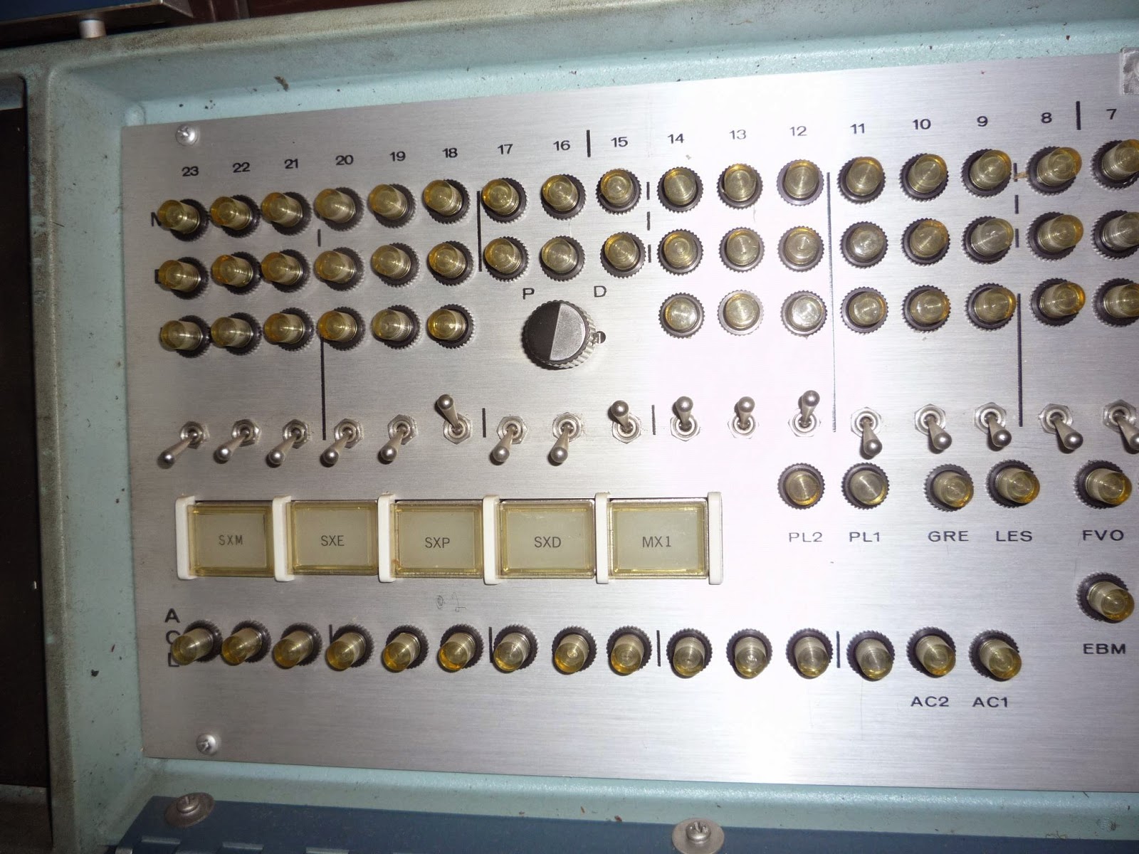
Honeywell 440


Front panel from a Honeywell 440.

Here is bitsavers documentation for a Honeywell 400, which seems to be a 48 bit device.  This panel shows two 24 bit registers, so may be the same device. The manual is for the system assembler.

http://bitsavers.trailing-edge.com/pdf/honeywell/h400/H400_EASYII_Feb62.pdf


Minimum system PDP 11


Minimum card / component count PDP 11 system, and monitor to attach to video card.